VRM Communication – Laptop Modding Adventure – Part 2/5
YouTube video transcription
[Original source] Partially based on the script of my YouTube videos: https://www.youtube.com/watch?v=sYzRqFkIQWc
[Updated] Contains updated data from 2022.
This guide is compatible with the the following laptops.
[Laptop] XMG Apex 15 Max (2022) with B550 chipset & XMG Apex 15 (2020) with B450 chipset
[Barebone] Clevo NH50VR / NH55VR / NH57VR / NH58VR (B550) & Clevo NH50AF1 / NH55AF1 / NH57AF1 / NH58AF1 (B450)
[Similar laptops] One K56-AR, Eluktronics Thicc-15, Eurocom Nightsky ARX15
[CPU] Zen3 & Zen2 Ryzen Desktop CPUs
[Note] This guide is applicable for Zen3 and Zen2 Ryzen CPUs in the B550 chipset based XMG APEX Max (E22) and B450 chipset based XMG APEX (E20) laptop.
Hi and welcome to part 2 of our little laptop GPU modding adventure. As I told you in the first part I will attempt to talk to the VRMs directly in this video and to do so we need to solder some wires onto the board.
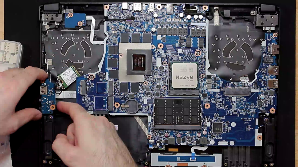
First things first we need to disassemble the laptop of course. So let’s watch it in timelapse so you don’t get bored.
One thing I want to notice is that you should not detach the keyboard so late into the disasembly process like me. I forgot to and had troubles to get it out without bending the whole case. Luckily nothing broke and we can go on with the soldering part.
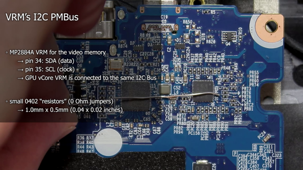
To communicate with the I2C Bus we need to solder three wires to some components on the board. I looked for possible connection points next to one of the two GPU related VRM controllers. I found a pair of zero Ohm jumper resistors which connect the controller’s I2C Bus to the board’s one. They are in a good location at the edge of the board to make soldering and insulation easier.
An easier location is good because the jumpers we want to work with are just 1 by half a millimeter in size. Or in imperial units 0.04 by 0.02 inches.
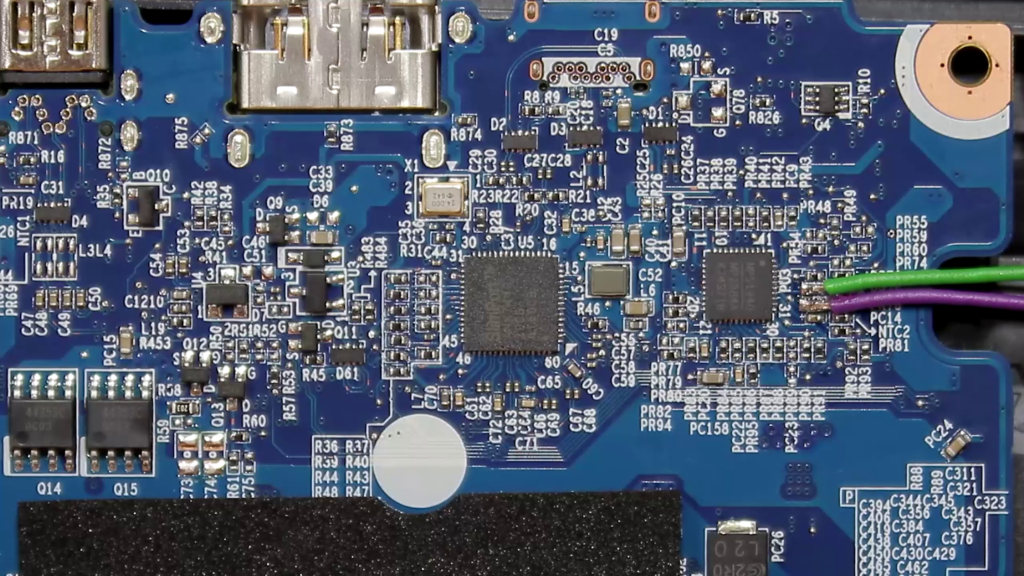
The first two wires you can see me soldering on are for the I2C itself. At first I tried to work with solid core wires because I thought they could be easier to fix to the other side of the board so they don’t move around. But I completely underestimated the stress they put on the soldering joints. So in the end I went back to the classic stranded wires.
The green wire got attached to the clock signal and the purple one to the data line. The black wire is ment to get the ground potential of the laptop only. I chose a point which is close enough to our I2C wires so i can make it look a bit tidier.
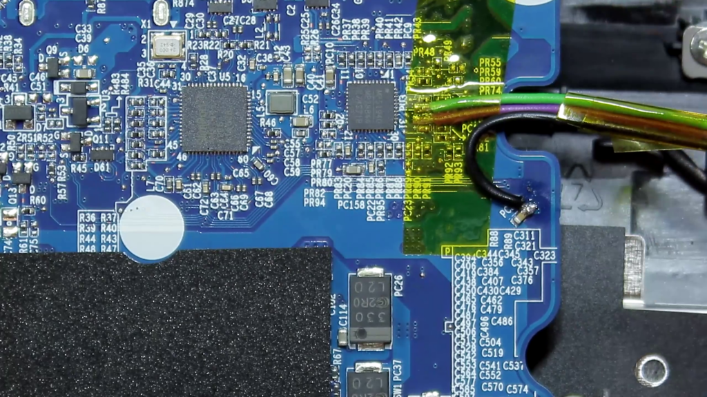
What’s left is to reassemble the laptop and test if we messed up or not. Because nothing blowed up, the laptop runs stable and the EVC software detects two VRM controllers I can finally say that it works flawlessly.
As you can see in the EVC software we get very detailed informations about voltages, current, power usage, efficiency and temperature. The temperature shown in the software is the highest internal junction temperature reported by an individual MosFET connected to the controller. And this gives us the opportunity to record stock baseline data including the VRM temperatures to see what the upcoming modifications to the laptop will change.
The most critical question we can answer now is: Do the VRMs got enough temperature headroom to handle a higher power draw from the GPU? Well the VRM temperatures I measured was 87°C for the GPU core VRM and 82°C for the video memory VRM in timespy.
But timespy doesn’t have a high load on the CPU simultaneously like real games do. And we already know that the GPU core VRM need to share it’s coldplate with the CPU core’s VRM. That means we should expect higher temperatures when we play real games. And it proved to be true.
Running Cyberpunk 2077 we can clearly see that the VRM temperatures for the GPU core reaches 95°C while the video memory VRM stays in the same temperature range as before since it’s not connected to the heatsink.
What’s also interesting to see is how much power really is delivered to the GPU die after the switching losses. ….
Typical overlays report an overall GPU power draw of 115W in our laptop, which includes the GPU core with roughly 90W and 25W for the other stuff like video memory and IO. The 90W shown in those overlays are measured before the VRM. Including the switching losses and an efficiency of about 87% we get 79W of usable power for the GPU core die effectively.
And finally it’s also interesting to take a look at the currents. In the last video I told you that the GPU draws roughly 110A, but I forgot about the switching losses. In reality we draw only 90A, which means we have plenty of headroom for the upcoming modifications on the current side.
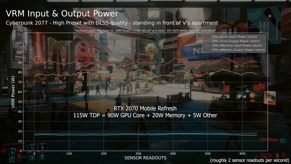
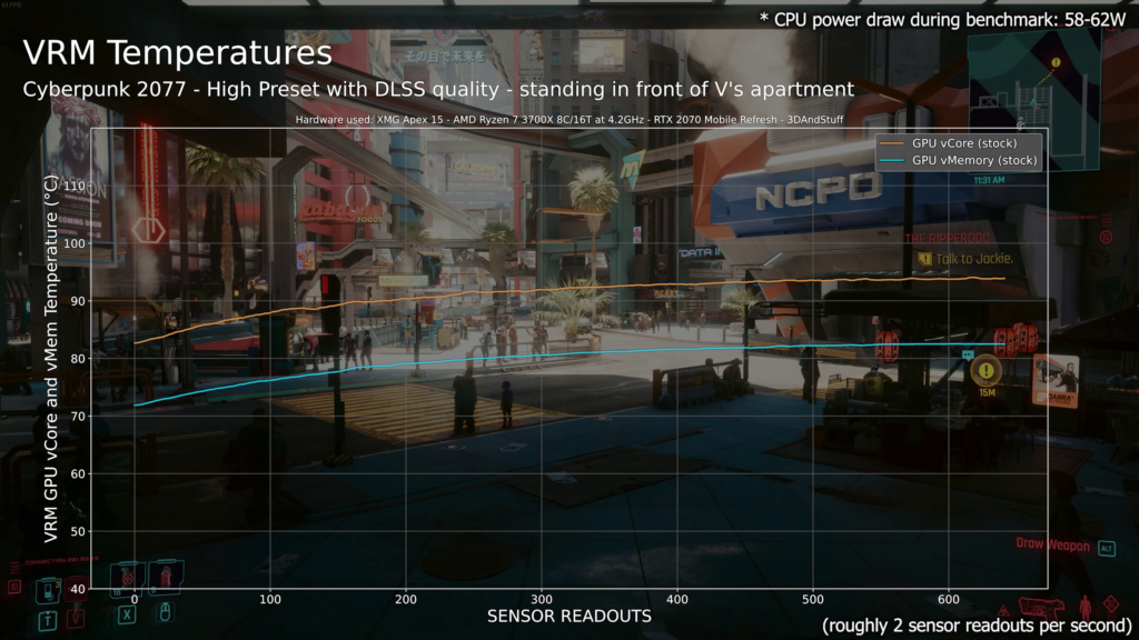
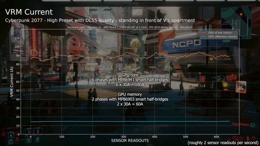

Looking at all the gathered data I think that a total of 140W power draw will be no problem for the laptop’s hardware. BUT we should improve the GPU core VRM temperature as much as possible to gain some more headroom, since 95°C VRM temperature is already quite high. Our MP86941 VRMs in general have an overtemperature protection which kicks in at 135°C as you can see in the EVC2 software. But running them at such high temperatures can’t be considered as healthy. Buildzoid made a video about VRM temperatures in 2018 and he said that 110°C is nothing to worry about, but for 24/7 usage he would suggest to go for 95 or even 85°C.
So all in all I should modify the heatsink in a way the VRM temperatures can be improved significantly. The cleanest way would be to remove the VRM coldplate completely and replace it with my own design. With the modified heatsink, the goal should be to stay under the said 110°C VRM temperature. I will also try to experiment with different thermal pads and see what difference they can make with the original and modified heatsink. And when the modified heatsink is working as expected I can go for the Shunt mod. …
Oh and remember me in the last video talking about using the I2C to set the power limit? Yeah well, I was totally wrong about that. It’s not possible with NVidia GPUs since they measure their power draw themself using shunt resistors. It’s true that you can force the VRMs to deliver a higher GPU voltage, but the GPU will throttle down the clock anway as soon as you hit the power limit. So in the end we have to do the shunt mod, otherwise there is no chance to exceed the fused power limit of 115W.


