Upgrading a soldered laptop GPU – Part 1
YouTube video transcription
[Original source] Partially based on the script of my YouTube video.
This guide is compatible with the the following laptops.
[Laptop] XMG Apex 15 Max E22 (2022) with AMD B550 chipset and AM4 CPU socket
[Barebone] Clevo NH50VR / NH55VR / NH57VR / NH58VR (B550 chipset)
[CPU] AMD Ryzen 7 5800X3D – Zen3 Ryzen Desktop CPU
[Note] This guide is applicable for almost all laptops. In general you can upgrade within the same GPU generation (e.g. RTX 3060 to RTX 3080), because the same pad layout is usually used for many different GPUs. But as I said: within the same generation.
You can upgrade the following. All GPUs in between included.
| From | To | Certainty | Comment |
| GTX 1650 Mobile (TU117) | – | high | no upgrade possible. Physically smaller GPU substrate and different pad layout. |
| GTX 1660 Mobile (TU116) | GTX 1660 Ti (TU116) | high | |
| GTX 1660 Mobile (TU116) | RTX 2080 Super Mobile (TU104) | uncertain! | should work, but have to try that to make sure. The VRMs of the laptop can’t handle the RTX 2080 (150W) though. However, RTX 2070 Mobile (115W) should be fine. |
| RTX 2060 Mobile (TU106) | RTX 2080 Super Mobile (TU104) | high | includes RTX 2070, 2070 Super Mobile GPUs |
| RTX 3060 Mobile (GA106) | RTX 3080 Ti Mobile (GA103) | high | includes RTX 3070, 3070 Ti and 3080 Mobile GPUs |
| RTX 4060 Mobile (AD107) | RTX 4070 Mobile (AD106) | high | upgrade to RTX 4080 and 4090 Mobile not possible due to different pad layout |
| RTX 4080 Mobile (AD104) | RTX 4090 Mobile (AD103) | high |
Intro
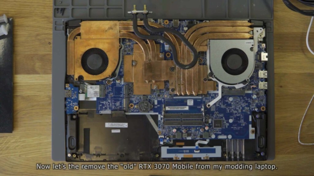
Besides the idea behind Framework, there are no modern laptops, which allow a CPU or GPU upgrade. Take my laptop for example. Even if the CPU is a socketed desktop processor and can be upgraded, the GPU is soldered and tops out at the mid-tier RTX 3070 Mobile for this model.
Unfortunately, soldered GPUs can’t be upgraded.
Let’s change that.
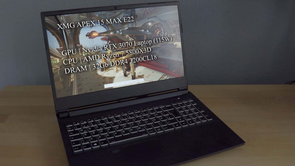
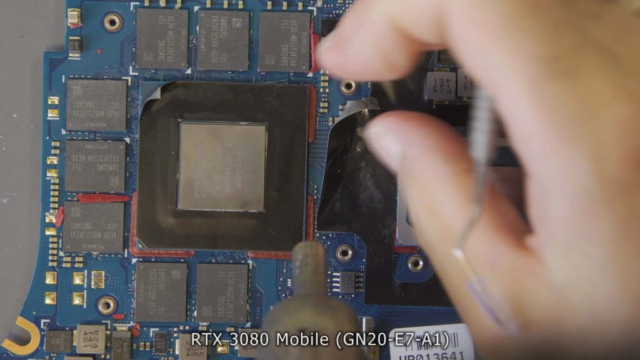
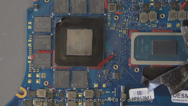
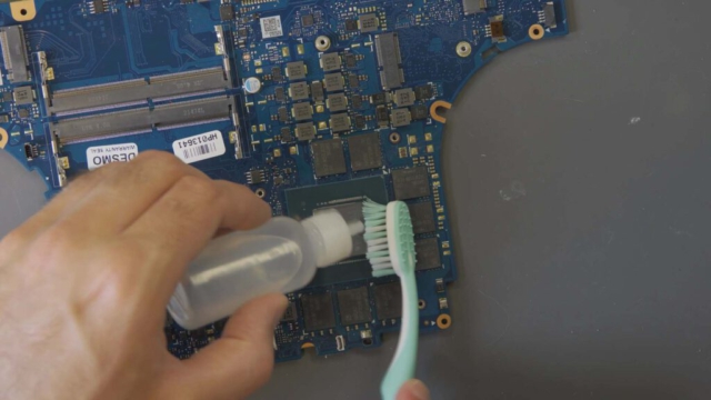
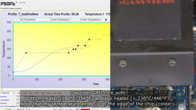
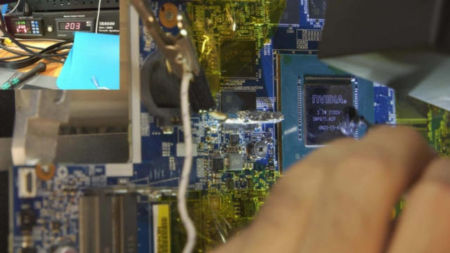
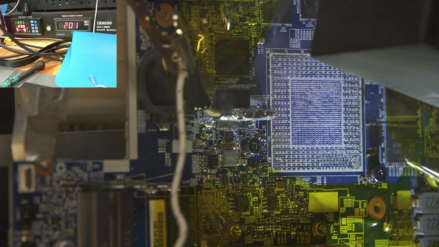
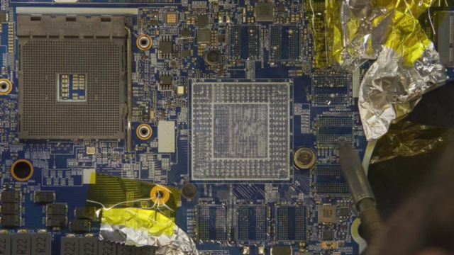
Here are some impressions from the YouTube video. If you want to know more about the solder process visit my second blog post, or watch Part 2 “Upgrading a soldered Laptop GPU – RTX 3080 Ti Mobile – Part 2”
And my laptop … got no image.
Luckily the laptop was still booting, so I could use diagnostic tools and a remote desktop connection as shown in my previous video about vBIOS crossflashing.
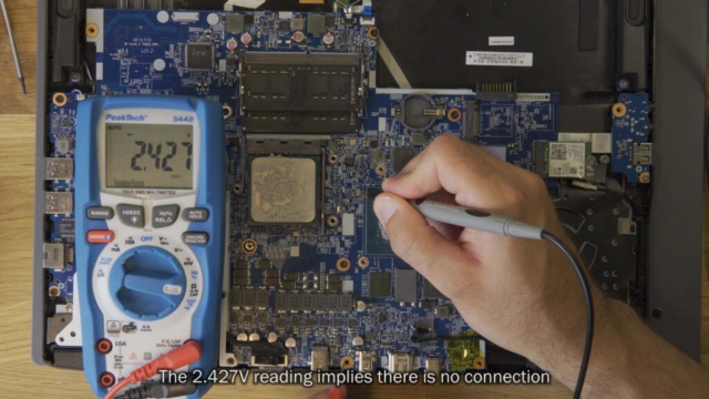
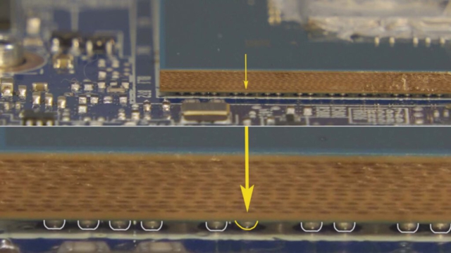
I soon realized that regardless of which vBIOS was flashed, I always received no vBIOS information. When I measured the diode voltage with reversed probes on the vBIOS flash chip, I noticed that the data output line had suspiciously high readings. Upon inspecting the solder connections near the GPU core, it became clear that the solder ball related to this signal was disconnected from the board.
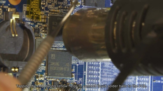
To address this, I reflowed the GPU AGAIN and gently tapped the edge of the disconnected solder ball. After this, the GPU was able to read the vBIOS, and the laptop finally displayed an image.
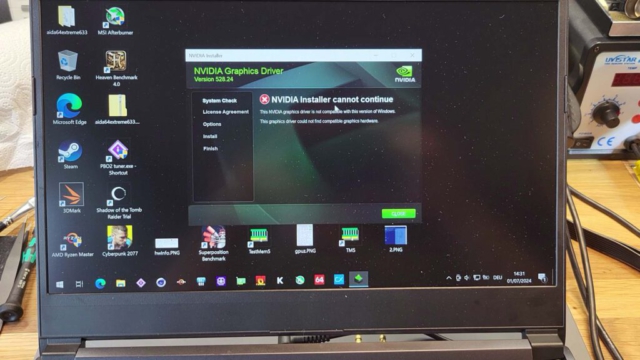
In Windows, the original Nvidia graphics drivers couldn’t be installed, which is expected since this specific hardware configuration doesn’t exist in Nvidia’s database. Unlike desktop computers, where you can simply swap the GPU and the driver installer will work, this process is more complex.
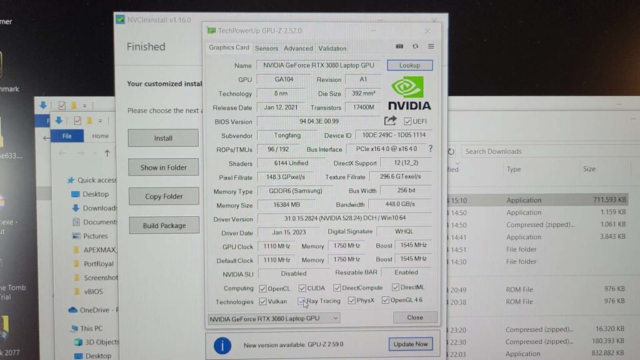
At this point in the project I had a chat with Prema and he told me about nvcleanstall, which is a tool, which basically mods the Nvidia installer’s files to accept the modified hardware.
Using that tool installation of the graphics driver wasn’t a problem anymore. So, thanks a lot Prema!
Before going into the details and questions you might have, let’s talk about the performance differences between the former RTX 3070 and 3080 Mobile GPUs.
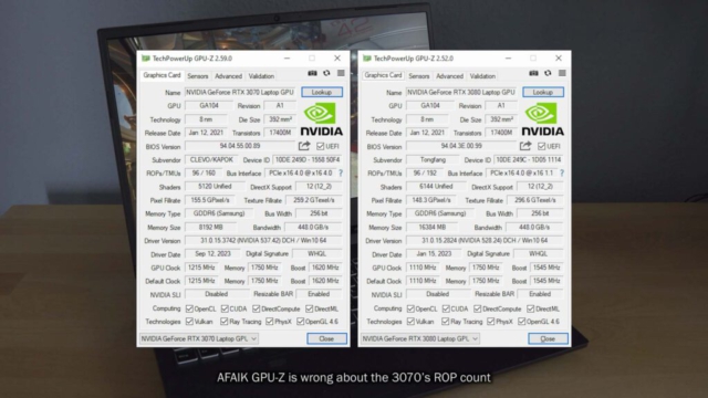
Both Laptop GPUs are based on the same GA104 GPU, but the 3080 Laptop variant got 20% more of everything: Shaders, TMUs, ROPs, Tensor cores and RT cores. Only the Level2 cache is the same.
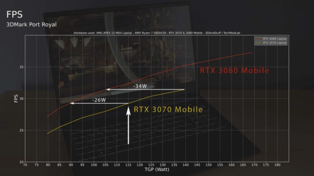
Hence only a look at the FPS differences at the same power draw makes sense.
As you can see the 3080 Mobile is more efficient than the 3070 Mobile. If you take a look at the performance at 115W of the former 3070 Mobile you can see that the 3080 Mobile performs the same at just 90W.
For the performance of the 140W 3070 Mobile on the other hand the 3080 Mobile only needs 105W.
On average, the 3080 Mobile does perform 11.5% better at the same power draw.
Okay, now let’s talk about the details of the GPU upgrade process.
And let’s start with the elephant in the room.
Were there more problems than those shown so far?
Oh yes, absolutely!
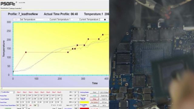
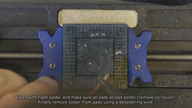
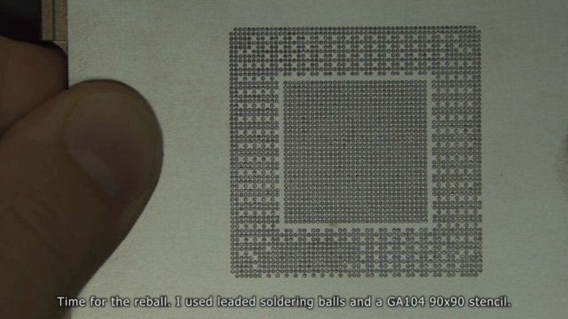
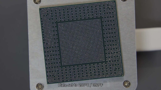
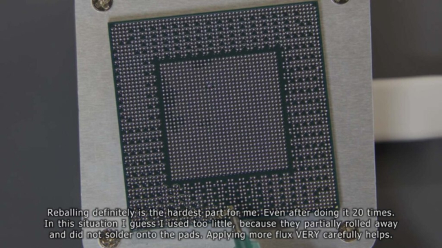
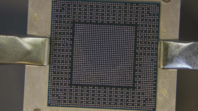
I had to reball the GPU core a total of four times! I already mentioned it briefly in the subtitles: For me personally, reballing is the hardest part and despite practice I still find it difficult not to get any solder bridges when melting the solder balls.
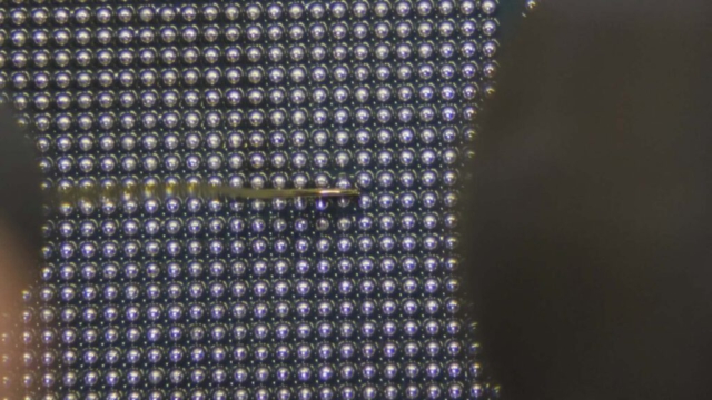
Today, after viewing the recordings, I noticed that the first solder balls still fuse well, but the last ones don’t fuse at all. This means that the flux has already evaporated by the end. That’s why adding a lot of flux after reaching the melting temperature worked, as I have shown in the first part of the video. But if I use more flux from the beginning, the solder balls float away when I heat up the GPU core and stick together. To make matters worse, some of the solder pads still had a little too much solder residue on them, which made the solder balls want to drift to the side as well.
I then took a two-week break before the next reball attempt, got better tools and practiced the knife technique for separating solder bridges.
Then came the finally successful reball. After positioning the solder balls, I wanted to lift the chip onto the mini heating plate. This time I had a good feeling. The chip was more carefully cleaned of solder than before and the amount of flux just felt right this time.
Well. But I dropped the chip.
Taking a deep breath, I inspected the damage and decided to correct the displaced solder balls manually.
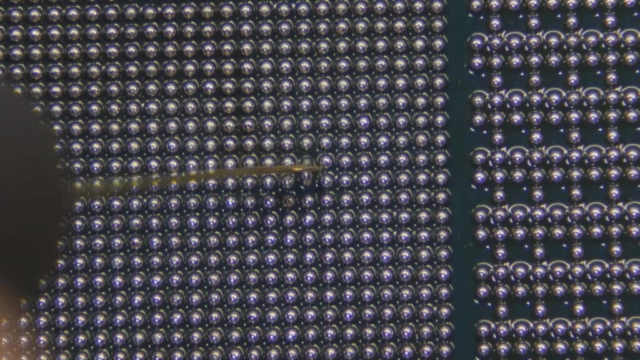
This took just under 20 minutes, but it was successful. And as you can see, the reflow with the addition of flux worked in the end and I was able to successfully separate the three solder bridges that had formed with the knife technique.
In the end, I still wonder if the large number of thermal cycles might have cost the GPU core some stability during overclocking. But that’s impossible to answer.
Two things were neglected in the video montage because they simply need more explanation. The Straps and the resistances of the power supplies.
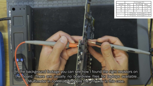
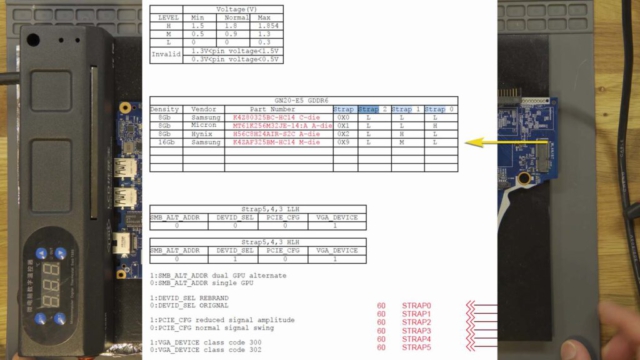
The straps are 6 signals that go to the GPU and can be set to three states each. Binary high, low and middle are set via small resistors. The high signal is reached when the voltage on the strap signal is pulled up to 1.8V. Low when it is pulled to ground and Middle when two resistors are set, one to ground and one to 1.8V.
They determine the configuration in which the GPU runs, including the video memory. To find out the right combination, you can either look at the straps on a donor board with the right GPU on it, or you can find schematics of your graphics card online in various repair communities and take the configuration from the straps table.
In my case, I needed the low-mid-low combination right at the end of the table, to make the 16GB of Samsung VRAM work.
And now let’s talk about the resistances.
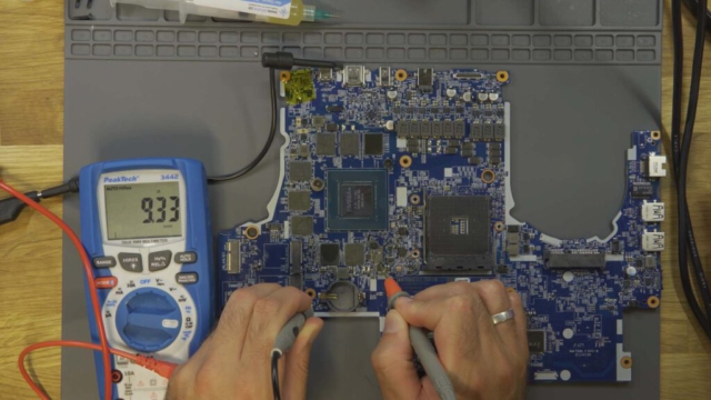
After soldering a chip, you should always check the resistances of the power supplies connected to the chip. This way you can detect short circuits that can damage components before you switch on the device for the first time.
In my case it was 26 Ohm on “VMem”, 10 Ohm on “Pex” and 200kOhm on 1.8V. “VCore” on the other hand is a hard one. Usually, it has a resistance of approximately 0.1 Ohm and is therefore difficult to measure. However, when I compared it with the resistance to ground using my multimeter in high-resolution mode, it was easy to see that this power supply does not have a short circuit either. The resistance is higher than the one to ground.
Does it make sense?
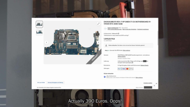
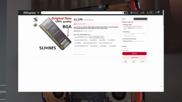
Well, the risk is immensely high and I really can’t recommend to pull it off. After all I got 11% more performance at the same 115W TGP configuration as before. But I paid 360€ for that. A very nice bonus is the 16GB VRAM instead of the former 8GB though, which will be useful for my use cases. However, I decided to spend another 90€ for the faster 16Gbit/s GDDR6 ICs, instead of reusing the 14Gbit/s ones from the donor board. If it was worth it I want to discuss in another video, where I want to take a look at overclocking of this GPU. The 14Gbit/s ICs however would’ve worked perfectly fine as well though.
When it comes to the question if it makes sense I can just say: no! Of course not.
I have just done it because I was curious if it is doable for me. Selling your old laptop and buying a newer one with a faster GPU is in almost all cases the better idea.
But if you are still interested …
Well. First and foremost at least basic understanding of GPU repairs is required. Including basic GPU repair soldering skills, like swapping a VRAM chip. And in the end I can recommend at least 10 reballs on a dead GPU core to practice your skills for the actual GPU core swap.
So yes, it is not an easy job and is not easy to learn. But I think the video shows that it is not impossible to upgrade a soldered laptop GPU, it is just VERY hard to pull off for the regular tech enthusiast. But there are people who repair GPUs daily and they could do it for you as well. It is a bigger financial risk though, compared to desktop computers, because if it fails, the whole laptop mainboard needs to be replaced, which basically is 90% of the cost of a laptop.
Additionally not all laptops accept a different GPU, or do not play well with a non-original vBIOS, because it is heavily linked to a piece of vendor specific software. In this case you could loose telemetry or power switching functionalities for example.
Well I think I have talked about the most important stuff. If you have more questions, don’t hesitate to write a comment.
That’s it for the video. Nothing more to say than: Thanks for watching!

